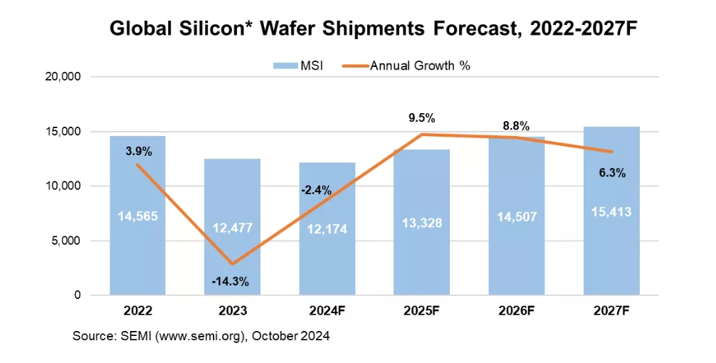
SEMI recently reported in its annual silicon wafer shipment forecast that global silicon wafer shipments are expected to decline by 2% to 12.174 billion square inches (MSI) in 2024, with a strong rebound of 10% to 13.328 billion square inches (MSI) in 2025 as wafer demand continues to recover from the downturn cycle.
SEMI expects that silicon wafer shipments will continue to grow strongly until 2027 to meet the growing demand related to artificial intelligence (AI) and advanced manufacturing, thereby driving increased utilization of global semiconductor capacity in wafer fabs. In addition, new applications in advanced packaging and high bandwidth memory (HBM) production require additional wafers, which also intensifies the market demand for silicon wafers. This type of application includes temporary or permanent carrier wafers, intermediate layers, separating devices into small chips, and separating memory/logic arrays.

Silicon wafers are the basic building material for most semiconductors, and semiconductors are an important component of all electronic devices. This highly engineered thin disc can have a diameter of up to 300mm and can be used as a substrate material for manufacturing most semiconductor devices or chips.
SEMI pointed out that all data cited in the report include polished silicon wafers and epitaxial silicon wafers shipped by wafer manufacturers to end-users, and do not include unpolished or recycled wafers.


